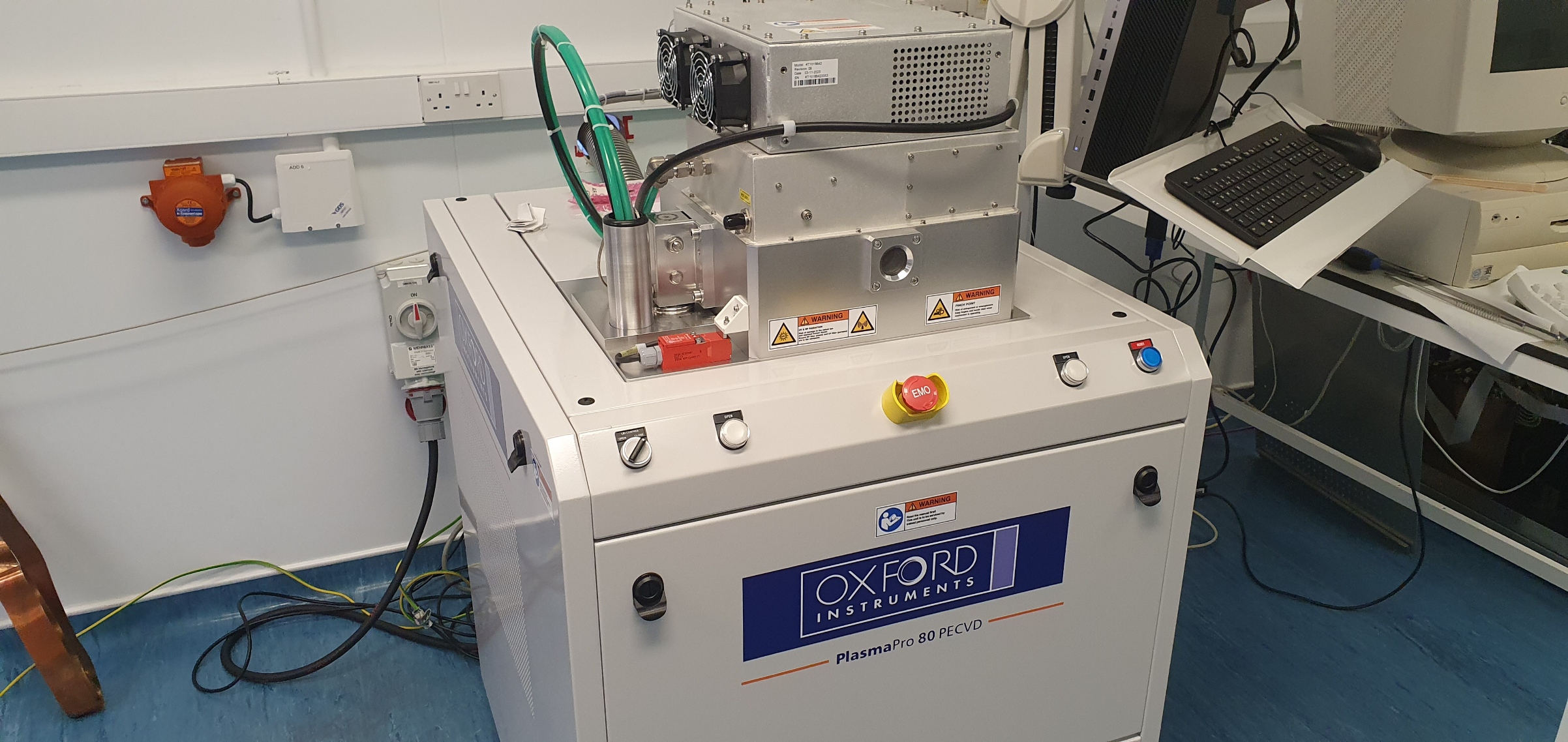
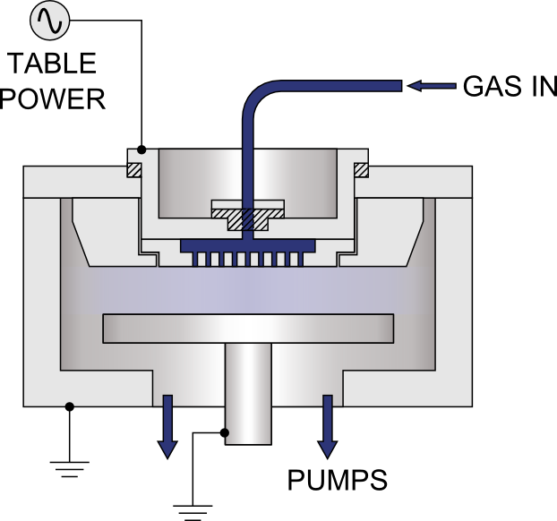
Plasma Enhanced Chemical Vapour Deposition (PECVD) is a well-established technique for the deposition of a wide variety of films. It can create high-quality passivation layers and high-density masks. This compact, small footprint system offers an open load design, allowing fast wafer loading and unloading. It enables high-performance processes using optimised electrode cooling and excellent substrate temperature control. Typical applications include high-quality deposition of silicon nitride and silicon dioxide for photonics, dielectric layers, passivation, etc., and hard mask deposition and etch for high brightness LED production.
Specifications:
- Open load design
- Excellent etch control and rate determination
- Excellent wafer temperature uniformity
- High pumping speed and excellent base pressure
- Up to 200 mm wafers
- Built to Semi S2/S8 standards
- Addition of <500 ms data logging
- Fault and tool diagnostics via front end software
- Rate: ~15 min for 1 um (for silicon nitride)